Engineering
Altek’s team of engineers are available to help customers succeed.
Altek’s onsite Engineering team provides electronic assembly engineering support. Our team is what sets us apart from the competition. We provide PCB layout and manufacturing evaluation to ensure a smooth process for your product build. The engineering team works closely with our Document Control and Process Documentation teams to ensure that no detail is overlooked.
What makes us different
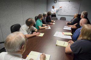
THE ENGINEERING TEAM
Our engineering team consists of electronic, software, mechanical, test, component, process, and manufacturing engineers. This team reviews your drawings, provides analysis and support, develops the process protocol for your build and consistently evaluates new equipment to maintain our leadership position in the Electronic Assembly Industry.
> See what our customers are saying about us.
Support
ENGINEERING SUPPORT
We provide support for PCB layout for new products, product updates, and component obsoletion or lead-time mitigation. We are a resource to take your PCBA or Box Build products, to prototype builds and full production, providing engineering support throughout all phases of the product lifecycle including aftermarket support.
Product Integrity
TESTING
Test is an important part of the electronic manufacturing process because it verifies that the product is going to work as intended in the application. Testing provides the ultimate peace of mind. Fixtures that automate part or all of the process can help mitigate the cost of test and reduce time and variation in the test process. If manual fixtures have already been developed, Altek can add a layer of automation to reduce time and cost. For example, as part of our continuous improvement process, and to meet a customer’s increase in demand, Altek developed an internal proprietary method of testing complex harness assemblies to reduce cost, increase throughput and improve quality. Our Engineers are on hand and ready to discuss your needs. Let us know how we can help you: “Contact an Engineer”
Keeping you informed
COMPONENT CHALLENGES
In this ever-changing component market, keeping up with parts availability and compatibility can be challenging. Yes, we have a component engineer who works with the team to resolve component issues to maintain high quality and reliability.
Getting it right
MANUFACTURABILITY ANALYSIS
Altek’s engineers are available to provide feedback on your design to confirm that it’s manufacturable and affordable. Simple things like tweaking the orientation of a component or keeping them away from the edge of the board can make a big difference in the cost of manufacturing. Making the best possible products for our customers is our priority. Please contact us for a “free” consultation as early in the design process as possible. “Contact an Engineer”
Our Process
MANUFACTURING YOUR PRODUCT
Altek utilizes a Digital Traveler system to ensure our operators have all the details needed to produce quality PCB assemblies consistently. It contains the instructions, materials, tooling, packaging, and even identifies the carton label. This keeps us efficient and running LEAN!
We are proud of what we do for our customers and always love to talk about it! So please… “Contact an Engineer”